1550 nm Semiconductor Optical Amplifier for Optical Communication, Fiber Sensing, LiDAR, and Test Systems
Part Number: ASOA1550N15D25GBT | March 2026
1. Introduction
Semiconductor optical amplifiers (SOAs) are becoming an increasingly important building block in modern photonic systems. As optical designs push for higher performance, tighter integration, and smaller footprints, the SOA's combination of compact packaging, broad gain bandwidth, and direct electrical controllability positions it as a practical and versatile amplification solution.
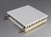
The ASOA1550N15D25GBT from Analog Technologies, Inc. is a 1550 nm SOA designed for demanding applications in fiber optic communication, distributed sensing, LiDAR, free-space optical links, and optical test and measurement systems. It delivers 25 dB of typical small-signal gain, up to 15 dBm output power, and a 100 nm gain bandwidth (−3 dB), all within a compact butterfly package that integrates a built-in TEC and thermistor for stable thermal management.
2. Key Specifications
| Parameter | Specification |
|---|---|
| Working Wavelength | 1550 nm (ASE center: 1515 nm) |
| Small-Signal Gain | 25 dB (typ) @ If = 250 mA, Pin = −5 dBm, 1550 nm |
| Maximum Output Power | 13 dBm (typ) / 15 dBm (max) @ If = 250 mA, Pin = +5 dBm |
| Gain Bandwidth (−3 dB) | 100 nm |
| Noise Figure | 7-9 dB @ 1550 nm |
| Polarization Dependent Gain | ≤ 2.0 dB (typ 1.0 dB) |
| Extinction Ratio | ≥ 50 dB (If on/off) ≥ 70 dB (negative bias) |
| Operating Current | 250-400 mA |
| Forward Voltage | 1.3-1.5 V |
| TEC Voltage (max) | 3.4 V |
| TEC Current (max) | 1.8 A |
| Thermistor Resistance @ 25°C | 10 kΩ typ (9.5-10.5 kΩ) |
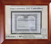
| Total Power Consumption | ~4 W (including TEC) |
| Operating Temperature | −10°C to +70°C |
| Package | Butterfly |
| Compliance | RoHS & REACH |
3. Optical Gain and Output Power
The ASOA1550N15D25GBT provides 25 dB of typical small-signal gain at 1550 nm, measured at an operating current of 250 mA with an input signal of −5 dBm. This gain level is well suited to amplification tasks ranging from boosting weak sensor return signals to compensating for insertion loss in complex optical assemblies.
Maximum output power is 13 dBm typical and up to 15 dBm, measured at an input level of +5 dBm. These two figures are measured under different conditions: the 25 dB gain applies in the small-signal (unsaturated) regime, while the 13 dBm / 15 dBm output corresponds to saturated operation. Designers should account for this distinction in link budget calculations.
The 100 nm gain bandwidth (−3 dB) centered near 1550 nm provides flexibility in wavelength allocation and accommodates channel drift, coarse WDM spacing, or broadband ASE-seeded configurations.
4. Noise Figure and Polarization Performance
The noise figure of 7 to 9 dB at 1550 nm is consistent with typical SOA performance at this wavelength. While higher than the 4-5 dB of gain-clamped EDFAs, it is fully acceptable in booster and inline amplification stages and in most sensing and instrumentation applications. For pre-amplification of very weak signals, this noise figure should be included in sensitivity and link budget analysis.
Polarization dependent gain (PDG) is ≤2.0 dB with a typical value of 1.0 dB, making the device suitable for standard single-mode fiber systems. For applications requiring strict polarization insensitivity, polarization-maintaining fiber coupling or a polarization scrambler should be considered.
5. Extinction Ratio and Optical Gating
The ASOA1550N15D25GBT achieves an extinction ratio of ≥50 dB by switching the drive current on and off, and ≥70 dB with a negative bias applied. These values confirm that the SOA can simultaneously act as a high-speed optical gate or shutter in addition to providing optical gain.
In fiber sensing applications, the SOA can replace an acousto-optic modulator (AOM) for signal chopping or pulse gating, eliminating a separate and costly modulation component. This dual function - amplification plus gating in a single device - simplifies system architecture, reduces component count, and lowers total system cost in sensing and time-domain measurement applications.
6. Thermal Management
The ASOA1550N15D25GBT integrates a built-in TEC (thermoelectric cooler) rated at up to 3.4 V and 1.8 A, together with a 10 kΩ (typ) NTC thermistor for closed-loop temperature feedback. The TEC maintains the SOA chip at a stable operating point, which is essential for reproducible gain, stable output wavelength, and long device lifetime. The thermistor output is compatible with standard ATI TEC controllers and other PID-based temperature control circuits.
The device is rated for operation from −10°C to +70°C ambient with approximately 4 W total power consumption including TEC overhead. For outdoor or wide-temperature deployments, supplemental cooling or an insulated enclosure should be evaluated alongside the on-board TEC.
7. Applications
7.1 Fiber Optic Sensing Systems
The high extinction ratio (≥50 dB on/off, ≥70 dB with negative bias) allows this SOA to perform optical amplification and pulse gating in a single component, replacing the AOM used for modulation or chopping in distributed temperature sensing (DTS), distributed acoustic sensing (DAS), and OTDR systems.
7.2 LiDAR and Wind Measurement Radar
In coherent LiDAR and Doppler wind-sensing systems, the ASOA1550N15D25GBT can serve as a booster amplifier for the transmitted optical pulse or as a pre-amplifier for the received return signal. Direct electrical control of gain and gating simplifies integration into pulsed LiDAR transmitters and reduces active component count.
7.3 Optical Communication - Pre-Amplification and Booster Amplification
The device is suited for booster and inline amplification in short- to medium-reach fiber links where an EDFA would be oversized or too costly. It can partially substitute for EDFA in cost-sensitive or space-constrained deployments, trading a somewhat higher noise figure for significantly smaller size, simpler drive electronics, and lower system cost.
7.4 Free-Space Optical (FSO) Links
The compact butterfly package and moderate power consumption are attractive for FSO terminal designs where SWaP constraints are common. Built-in TEC support enables stable operation across the temperature ranges typically encountered in outdoor FSO installations.
7.5 Optical Test and Measurement
As a wideband, gain-adjustable 1550 nm amplifier, this SOA is useful as a signal booster in optical network analyzers, component test benches, and coherent receiver evaluation platforms. Its 100 nm gain bandwidth supports multi-channel or swept-wavelength testing across a wide portion of the C and L bands.
8. SOA vs. EDFA: Practical Considerations
The table below summarizes the key differences between semiconductor optical amplifiers and erbium-doped fiber amplifiers to help designers select the right technology for their application.
| Attribute | SOA (ASOA1550N15D25GBT) | Typical EDFA |
|---|---|---|
| Size | Compact butterfly | Large module or rack unit |
| Pump laser | Not required | Required (980 nm or 1480 nm) |
| Noise figure | 7-9 dB | 4-5 dB (gain-clamped) |
| Gain switching | Nanosecond-scale | Millisecond-scale |
| Optical gating | ≥50 dB extinction | Not available |
| Cost | Lower | Higher |
| Integration | PCB / compact module | Bench / rack |
For system designers, the choice between SOA and EDFA depends primarily on the noise budget, physical size constraints, and whether optical gating functionality is required. The ASOA1550N15D25GBT is the stronger choice wherever compactness, switching speed, or cost efficiency is the priority.
9. Technical Notes
10. Ordering Information
| Field | Detail |
|---|---|
| Part Number | ASOA1550N15D25GBT |
| Package | Butterfly |
| Price | $1,399 |
| Datasheet | Download Datasheet (PDF) |
| Product Page | analogtechnologies.com/Semiconductor_Optical_Amplifier.html |
| Online Store | shop.analogtechnologies.com |
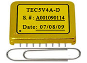
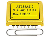
11. Recommended Laser Drivers: ATLS500MA104 and ATLS500MA103
For driving a seed laser diode or any diode laser at up to 500 mA in a photonic system built around the ASOA1550N15D25GBT, ATI offers two proven 500 mA constant-current laser drivers: the ATLS500MA104 and the ATLS500MA103. Both are housed in the same compact 6-sided metal DIP package with identical footprint and pin-out, and both deliver the low-noise, stable current that diode lasers and SOA-seeding applications require. The primary difference between them is noise performance: the ATLS500MA104 achieves lower output noise of less than 0.6 μARRMS at 0.1 Hz to 10 Hz, while the ATLS500MA103 is specified at ≤5 μAP-P over the same bandwidth. Both are well suited to DPSSL, EDFA, SOA, fiber laser, and sensing applications.
Key features shared by both models:
| Parameter | ATLS500MA104 | ATLS500MA103 |
|---|---|---|
| Max output current | 500 mA | 500 mA |
| Output noise (0.1-10 Hz) | < 0.6 μARRMS | ≤ 5 μAP-P |
| Modulation bandwidth | 4.67 MHz | 1 MHz |
| Rise / fall time | 75 nS | 170 nS |
| Shutdown / standby | 3-state SBDN pin | Single SDN pin |
| Soft-start | Yes | No |
| Loop good (LPGD) | Yes | Yes |
| Current monitor (LIO) | Yes | Yes |
| Temp monitor (TMPO) | Yes | Yes |
| Package | DIP / SMT | DIP / SMT |
| Price (1-9 pcs) | ~$59 | $59 |
Choose the ATLS500MA104 when the lowest possible noise is required. Choose the ATLS500MA103 when the application is less noise-sensitive and the wider 1 MHz modulation bandwidth or single-pin shutdown control is preferred.
| Resource | ATLS500MA104 | ATLS500MA103 |
|---|---|---|
| Product Page | ATI 104-series page | ATI 103-series page |
| Datasheet | Download ATLS500MA104 PDF | Download ATLS500MA103 PDF |
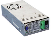
12. Recommended TEC Controller: TECA1-5V-3.5V-DAH
The ASOA1550N15D25GBT integrates a built-in TEC rated at up to 3.4 V and 1.8 A, paired with a 10 kΩ NTC thermistor. To drive this TEC for closed-loop temperature stabilization - or to regulate any TEC in the broader photonic system - the TECA1-5V-3.5V-DAH is the recommended ATI TEC controller. Powered from a standard 5 V supply, it provides up to 3.5 V across the TEC (covering the SOA's 3.4 V maximum) and up to 2.5 A output current, with a temperature stability of 0.004°C.
The TECA1LD-5V-3.5V-DAH variant (with the "LD" suffix) includes an internal compensation network pre-matched to butterfly-packaged TEC thermal loads, reducing external component count and simplifying PCB design when driving SOA-style packages.
Key features:
| TECA1LD-5V-3.5V-DAH - Pricing | Unit Price (USD) |
|---|---|
| 1-9 pcs | $89.00 |
| 10-49 pcs | $86.00 |
| 50-199 pcs | $83.00 |
| 200-499 pcs | $80.00 |
| ≥500 pcs | $77.00 |
| Resource | Link |
|---|---|
| Product Page (TECA1 series) | analogtechnologies.com/TECA1-xV-xV-DAH.html |
| Datasheet (PDF) | Download TECA1-xV-xV-DAH Datasheet |
| Buy TECA1LD-5V-3.5V-DAH | shop.analogtechnologies.com - $89 / unit |
| Evaluation Board TECEV104 | analogtechnologies.com/tec-controller.html |
For More Information
Analog Technologies, Inc. • 1161 Ringwood Ct., #110, San Jose, CA 95131, U.S.A.
Tel: 408-748-9100 • www.analogtechnologies.com