|
Thermoelectric Cooler Controller Design Made Simpler
Gang Liu, Can Li and Fang Liu, Analog Technologies, Inc.
Feb. 1, 2013 — TEC controller design experts offer tips to lower the cost and simplify the
design of the devices, and to increase their ease of use.
Thermoelectric cooler (TEC) controllers are becoming more prevalent in thermal management
designs because they can drive a thermoelectric cooler to stabilize the temperature of laser diodes or passive components used in communications equipment.
TECs have several advantages for temperature regulation: high accuracy and stability, fast response time, a wide set-point temperature range, and a simple structural design with no moving parts. Also, they are small and lightweight, reliable, noise-free and environmentally friendly. However, when comparing with temperature regulation approaches based on heat sinks or compressors, for applications requiring especially high thermal power output, TECs may have certain shortcomings: low efficiency, low thermal power, high cost of both TECs and controllers,and complex controller designs.
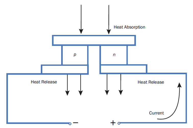
Figure1. Thermoelectriccoolers(TECs)arehighlyaccurateand stable for temperature control, with a wide set-point temperature range and a simple packaging design with no moving parts. They are small and light, highly reliable, noise-free and environmentally friendly. Here, a structuraldiagramof a TEC.
Cold/hot sides and +/- terminals
In 1834, French physicist Jean-Charles Athanase Peltier found that the junctions of dissimilar metals are heated or cooled depending upon the direction in which an electric current passes
through them. This effect became the Peltier effect.
A TEC has two ceramic plates with Peltier elements sandwiched in between. Based on the Peltier effect, these elements produce heat and cold by injecting an electric current through them. All the Peltier elements are connected in series; the first and last are each connected to a separate wire terminal. The plate on which the two terminals are mounted is often called the hot-side plate or simply the hot side; the other side is designated the cold-side plate or the cold side. The two sides are symmetrical in terms of thermal functionality, but the thermal load of the side with the terminals is a little higher because of the wire leads.
A DC current is injected into the TEC through the two terminals, and this generates a temperature difference between the two plates: One plate becomes cooler, while the other side becomes warmer.
When the cold side cools down, the TEC terminal connecting the positive lead of the power supply is designated as the plus (+) terminal, or the positive lead of the TEC; the other is designated as the minus (-) terminal, or the negative lead. As the DC current reverses direction – i.e., flows out from the plus terminal – the cold side will heat up and the hot side cool down.Therefore, TECs can be used both for cooling down and heating up the thermal load.
TECs can’t “generate” cold; they only move heat from one side to the other. They “produce” heat more efficiently than cold under the same size or current conditions because not all of the electric energy of the DC current is used for removing the heat; some energy is consumed by the Peltier elements and converted into heat, which is conducted to the two sides of the TEC at the same time. This heat boosts the heating-up power of the TEC but makes the cooling-down function less efficient.
To achieve precise control of the thermal load temperature, proper design of the TEC controller is critical.
TEC-based systems: five key components
To form a TEC-based temperature control system, a thermal load – the temperature of which must be controlled – is mechanically and thermally mounted on the cold side. There are five key components in a TEC controller: the temperature sensor, the sensor-conditioning circuit, the error-sensing and amplification circuit, the compensation network and the output H bridge, all cascaded in series to control a thermoelectric cooler (Figure 2).
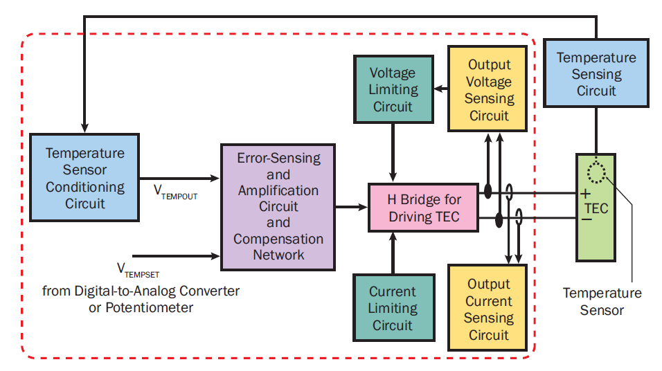
Figure 2. This functional block diagram of a TEC shows the five key components.
The error-sensing and amplification circuit measures the voltage difference between VTEMPOUT and VTEMPSET, which is an analog voltage representing the set-point temperature, and amplifies the difference to drive the output H bridge. Given the thermal mass and thermal resistance of the Peltier elements, the cold-side plate and the thermal load all cause delays between the time the DC current is applied and the time the thermal load changes its temperature; a compensation network is needed and implemented with the error-sensing and amplification circuit. Otherwise, the closed control loop would not be stable.
The H bridge circuit drives the TEC with a DC current, with the magnitude and direction precisely controlled by the error amplifier’s output voltage.
Temperature-sensing conditioning circuit
For most TEC-based application systems, a negative temperature coefficient thermistor (or thermal resistor) is used as the temperature sensor. Its resistance inversely varies with its temperature change in a nonlinear way – i.e, the resistance of the thermistor decreases as its
temperature increases. The most common value in diode laser TEC designs is 10 KΩ. The resistance change is then sensed and converted into an analog voltage,VTEMPOUT, by the temperature sensor conditioning circuit. The main functions of this circuit are to amplify the signal received from the temperature sensor and to linearize T (temperature) vs. V (voltage) curve.
A typical measurement circuit is shown in Figure 4. It amplifies the temperature signal and linearizes the variation relationship between the input temperature and the output voltage, VTEMPOUT. Notice that the input signal is sent to the negative input of the amplifier. Thus, as temperature goes up, so does output voltage.
By properly calculating the resistors (R1, R2, R3, R4 and R5), the variation of the output voltage,VTEMPOUT, is almost linear to the thermistor’s temperature. Calculation details can be found atwww.analogtechnologies.com.
Applications requiring low drift and small absolute errors could benefit from another type of
temperature sensor called a resistive temperature device, a platinum resistor-based instrument.
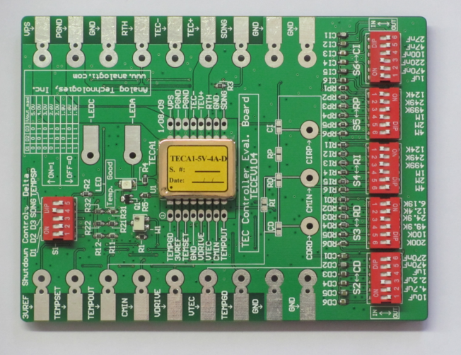
Figure 3. TheTEC controller on this evaluation board was designed by AnalogTechnologies Inc.
Error sensing and amplification circuit
This is a critical component for minimizing temperature error and ensuring temperature stability. It detects the error between the output voltage from the temperature sensor-conditioning circuit, which represents the measured thermal load temperature, and a set-point voltage from a digital-to-analog converter or a potentiometer, which represents the set-point temperature and amplifies the error to generate a signal for driving the TEC driver circuit, the H bridge. In Figure 3,a potentiometer is used to set the voltage at VTEMPSET.
The transfer function from the HB-DR output in Figure 4 to the thermal load temperature is of a less than second-order system that imposes significant phase delays between the input and the output.
The compensation network is needed to stabilize the thermal control loop, reduce TEC response time when the set-point temperature is changed, and minimize the temperature errors caused by disturbances imposed on the system so that the thermal load temperature remains equal to the set-point temperature.
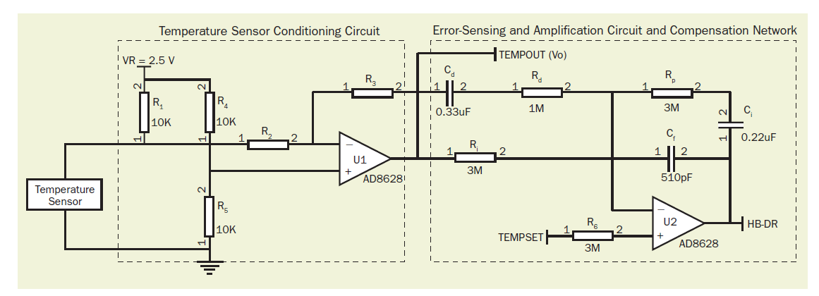
Figure4. A typical TEC control circuit comprises a temperature sensor conditioning circuit, an error amplifier and a compensation network.
These disturbances include thermal load change, such as changing the laser diode current if the diode is the thermal load, and TEC hot-side ambient temperature change, as when the speed of the cooling fan changes, or the air temperature changes where the TEC hot-side heat sink is placed.
There are many ways to compensate second-order systems. The compensation network shown in Figure 4 has the advantages of being simple and effective for TEC controls. Second-order system compensation is a broad and deep topic in control engineering; here, we can describe only briefly the basic functions of the components in the network.
Thinking in the frequency domain, Cd and Rd provide the signal path for the high-frequency
component in VTEMPOUT, while Rp provides the feedback path. The voltage gain is: Rp ⁄ Z(Cd 1 Rd).
Z(x) is the impedance of x; the cutoff frequency is set by Rd x Cd. For the low-frequency component in VTEMPOUT,
Ri provides the signal path, while Rp also provides the feedback path.The voltage gain is: Rp ⁄ Ri.
The upper cutoff frequency is set by Rd x Cd; the lower cutoff frequency is set by Ri x Ci. For the DC component, the gain is almost infinite (about 1 million), resulting in zero residual temperature error, except for the errors caused by the offset voltage and the current of the amplifier.
Cf is for eliminating the signals outside the useful frequency range – i.e., less than 10 Hz – so that the noise at the output voltage HB-DR is reduced.
After Cd, Rd, Ri, Rp and Ci are adjusted properly, the compensation network can match the thermal load properly so that the system can stabilize the temperature quickly and precisely. The values of the compensation network components shown in Figure 4 are typical of a value set for telecom laser modules, including pump and transmitter lasers.
In practice, because the transfer functions of the TEC thermal systems vary widely for different designs and applications, it is difficult to measure the transfer function and calculate the values of the compensation network. From our experience, the best way to tune the compensation network is by incorporating a tunable compensation network in the design.
The basic goal in tuning the compensation network is to minimize the overshoot and the settling time of the measured temperature as the set-point temperature changes.
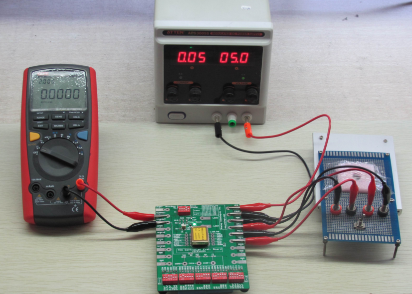
Figure5. A TEC controller application setup. The evaluation board allows fine tuning of the proportional integral derivative compensation network to match the thermal load and to stabilize the control loop.
Using the evaluation board seen in Figure 5, we can conduct experiments to find the function of the proportional integral derivative (PID) compensation network. A PID controller is a generic control-loop feedback mechanism widely used in industrial control systems. It calculates an “error” value of the difference between a measured process variable and a desired set point. The controller attempts to minimize the error by adjusting the process control inputs. To simulate a set-point temperature jump, we apply a small step function on the VTEMPSET, using an oscilloscope to see VTEMPOUT at the same time. Compensation network tuning waveforms are shown in Figure 6.
H bridge
The basic function of the H bridge is to provide a bidirectional current drive to the TEC so that the TEC can heat up and cool down the thermal load with precisely regulated output thermal power.
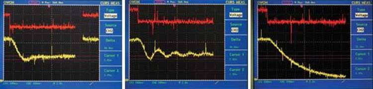
Figure6.These three figures show compensation network tuning waveforms: (left) Compensation networkproperlytuned.Red:VTEMPSET;Yellow: VTEMPOUT. Compensation network: Cd 5 270nF;Rd 5 6.19K; Ri 5 1.5M; Rpp 5 2.5M; Cii 5 100nF. (middle) Response has overshoot. Red: VTEMPSET;Yellow:VTEMPOUT.Compensation network: Cd 5 17uF; Rd 5 6.19K; Ri 5 1.5M; Rp 5 6.5M; Ci 5 100nF. (right) Response is too slow. Red:VTEMPSET;Yellow:VTEMPOUT.Compensationnetwork:Cd 5 0 (open circuit); RD = ∞ (open circuit); Ri 5 7.5M; Rp 5 124K; Ci 5 2uF.
The main technical merits of the H bridge are power efficiency, output voltage regulation range and drop-out voltage.
The power efficiency is defined as: (output power) / (input power). The dropout voltage is the voltage drop from the TEC controller input voltage to its maximum output voltage.
Because the H bridge takes up most of the TEC controller space and material cost, saving printed circuit board space is a major concern for designers.
In reality, most TECs require a driving current greater than 2 A, so H bridge efficiency is important. Conventionally, to make a high-efficiency H bridge, two switch-mode drivers are
needed.
A new method patented by Analog Technologies uses one switch-mode driver and one linear-mode driver to achieve higher efficiency in a smaller space with less noise and lower cost.
Voltage- and current-limiting circuit
Under the cooling mode, the TEC’s cooling power is maximized when its current reaches IMAX (the maximum current) and the voltage is simultaneously at the maximum value, VMAX.
Keep increasing the TEC current or voltage beyond this point and the TEC’s cooling power will keep going down until it completely disappears. For the TEC controller, the control loop polarity will be turned from negative feedback into positive feedback: The higher the thermal load temperature, the higher the TEC current and voltage. Also, the output cooling power from the TEC will be lower, and the thermal load temperature will be higher, although it is supposed to be lower.
This state is called thermal runaway, as shown in Figure 7. To prevent this, the TEC voltage and the current must be limited by the voltage- and current-limiting circuits. These two circuits clamp the output to the maximum values even as the error amplifier requires the output to go higher. The maximum output current and maximum output voltage are set by two respective analog voltages on a TEC controller and are often equal to the maximum current and the maximum voltage of the TEC, respectively. However, in some laser diode applications, the maximum heating current must be set lower than the maximum cooling current to limit the thermal load temperature and protect the laser diode.
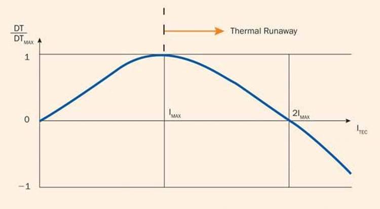
Figure7. A normalized TEC cooling power vs. current. When current is ,2IMAX,theTECcools down the thermal load; at .2IMAX, it heats up the thermal load.
TEC controller design
An optimal TEC controller should have the best combination of these major specifications: high temperature stability, high power efficiency, low AC ripple current at the output, low kickback ripple voltage to the power supply, easy interfacing and monitoring, a small printed circuit board area, fault detection, good temperature indication and low cost. To achieve such a design,trade-offs among major parameters must be made.
TEC controllers can be left alone or controlled and monitored extensively. The controlling and monitoring scales must be set according to system needs. The parameters that are frequently controlled are target temperature, maximum output current, maximum output voltage and TEC controller shutdown.
Monitored parameters are the following: actual thermal load temperature, TEC current, TEC voltage, “temperature good” indication and Seebeck voltage (the open circuit voltage of the TEC). For reliable system operation, it is important to have effective indication of system failures. To protect the TEC from open or short circuits of the thermistor and the TEC, limiting the output current and voltage is also important. Some off-the-shelf TEC controllers can readily be used to achieve high system performance without going through all the TEC design hassles.
Meet the authors
Gang Liu is president of Analog Technologies Inc. of Santa Clara, Calif., where he is also a design engineer; email: gang.liu@analogtechnologies.com. Can Li is the company’s design engineer as well as an undergraduate student in the department of microelectronics and nanoelectronics at Tsinghua University in Beijing; email: lican09@mails.tsinghua.edu.cn. Fang Liu works in application support at Analog Technologies; email: fang.liu@analogti.com.
|